July 27, 2026
10 min read
NVIDIA Vera CPU: Accelerating Electronic Design for Future Game Hardware
Key Takeaways
- •The Escalating Complexity of Modern Chip Design
- •Introducing the NVIDIA Vera CPU: A Catalyst for Chip Design
- •Strategic Collaborations: Cadence and Synopsys
As technical directors and senior developers, we constantly look ahead, anticipating the hardware capabilities that will define the next generation of games. The performance ceiling of our creations is intrinsically linked to the underlying CPUs and GPUs. In this pursuit of pushing graphical fidelity, simulation complexity, and AI sophistication, the speed at which these critical components are designed and brought to market is paramount. NVIDIA's recent advancements with their Vera CPU, specifically in accelerating Electronic Design Automation (EDA), represent a foundational shift that will profoundly impact the future of game development.
The Escalating Complexity of Modern Chip Design
The era of simple, monolithic chip designs is long past. Today's CPUs, GPUs, and specialized AI accelerators are intricate ecosystems of billions of transistors, complex logic blocks, and high-speed interconnects. Each new generation demands higher core counts, wider memory bandwidths, more sophisticated instruction sets, and increasingly specialized processing units for tasks like ray tracing or AI inference.
This relentless march of innovation, while exciting for end-users and developers, presents an immense challenge for chip designers. The sheer scale and complexity mean that manual design is impossible. This is where Electronic Design Automation (EDA) tools become indispensable. EDA encompasses a broad suite of software applications used to design, verify, and manufacture integrated circuits. From logical design to physical layout, simulation, and verification, these tools automate critical, time-consuming processes.
However, even with advanced EDA tools, the design cycle for a modern high-performance chip can span years. Each iteration of a design requires extensive simulation and verification to ensure functional correctness and performance targets are met. As chip complexity grows exponentially, the computational demands of these EDA workloads skyrocket, threatening to slow down the pace of innovation. This bottleneck directly impacts when and how much more powerful hardware becomes available to us, the game developers.
Introducing the NVIDIA Vera CPU: A Catalyst for Chip Design
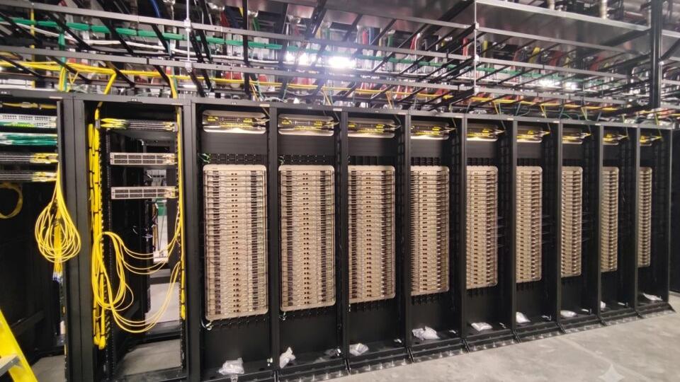
Recognizing this critical bottleneck, NVIDIA has taken a strategic step by deploying its own Vera CPU to accelerate the design of its next-generation CPUs and GPUs. The Vera CPU is not just another processor; it's specifically optimized to tackle the most demanding EDA workloads. This internal deployment signifies NVIDIA's commitment to self-sufficiency and pushing the boundaries of chip design efficiency.
The core idea is simple yet powerful: use advanced hardware (Vera CPU) to design even more advanced hardware (future NVIDIA CPUs and GPUs). This meta-optimization loop allows NVIDIA to significantly reduce the time spent on design iterations, leading to faster development cycles and ultimately, more powerful products reaching the market sooner.
Strategic Collaborations: Cadence and Synopsys
NVIDIA isn't going it alone. A key aspect of this initiative is the collaboration with industry leaders Cadence and Synopsys. These companies are titans in the EDA software space, providing the essential tools that chip designers rely on daily. By working directly with Cadence and Synopsys, NVIDIA is optimizing these critical EDA applications specifically for the Vera CPU architecture.
This partnership is crucial because generic CPU performance improvements don't always translate efficiently to highly specialized EDA tasks. Deep optimization at the software-hardware interface is required to extract maximum performance. This involves:
- Profiling and identifying bottlenecks: Pinpointing which parts of the EDA applications consume the most compute resources.
- Code optimization: Tailoring algorithms and data structures to leverage Vera's specific architectural strengths, such as its core count, cache hierarchy, or instruction sets.
- Parallelization: Ensuring that EDA workloads can effectively scale across Vera's multiple cores and threads, maximizing throughput.
The result of these collaborations is a synergistic effect where the Vera CPU's hardware capabilities are fully unlocked by highly optimized EDA software, leading to unprecedented acceleration in chip design.
Technical Deep Dive: Accelerating EDA Workloads
The source article highlights that Vera delivers a "significant boost in performance for demanding EDA workloads, including simulation, verification, and place-and-route." Let's break down why these specific stages are so critical and compute-intensive:
1. Simulation
Before a chip design can be physically manufactured, it must be extensively simulated to ensure it behaves as intended. This involves running complex models of the chip's logic and timing characteristics against vast sets of test vectors.
- Functional Simulation: Verifies that the chip performs its logical operations correctly. This often involves executing millions, if not billions, of simulated clock cycles.
- Timing Simulation: Analyzes signal propagation delays to ensure the chip operates reliably at its target clock frequency.
- Power Simulation: Estimates power consumption under various operating conditions, crucial for thermal management and battery life in mobile devices.
These simulations are computationally expensive, often involving iterative calculations across large data sets representing the chip's state. A faster Vera CPU can execute these simulations in a fraction of the time, allowing designers to run more exhaustive tests or explore more design variations.
2. Verification
Verification is arguably the most critical and time-consuming part of the chip design process, often consuming 70% or more of the total design effort. It's about ensuring the chip is entirely bug-free before fabrication, as fixing errors post-silicon is prohibitively expensive.
- Formal Verification: Uses mathematical proofs to confirm that a design adheres to its specification, guaranteeing correctness for certain properties.
- Emulation/Prototyping: Mapping a design onto reconfigurable hardware (like FPGAs) or specialized emulation systems to run real-world software workloads at near-real-time speeds, catching complex corner-case bugs that simulations might miss.
- Regression Testing: Running thousands of pre-defined test cases against the design after every change to catch unintended side effects.
The acceleration of verification with Vera CPU means that designers can achieve higher coverage faster, leading to more robust and reliable chips. This directly impacts game developers by providing more stable and predictable hardware platforms.
3. Place-and-Route
This is a physical design stage where the logical design is translated into a physical layout on the silicon wafer.
- Placement: Deciding the optimal physical location for each logic gate and memory block on the chip. This is a complex optimization problem, aiming to minimize wire length, reduce signal delay, and avoid congestion.
- Routing: Connecting all the placed components with electrical wires (interconnects). This involves navigating multiple metal layers and adhering to strict design rules (e.g., minimum spacing, wire width).
Place-and-route tools are highly sophisticated combinatorial optimizers. They explore an astronomical number of possible layouts to find the best compromise between performance, power, and area. Faster compute from Vera CPU allows these tools to explore more options, converge on better layouts more quickly, and handle increasingly dense and complex designs.
The following chart illustrates the traditional vs. accelerated EDA workflow and its impact:
Impact on Game Development
So, what does this highly technical, behind-the-scenes chip design optimization mean for us, the game developers? The impact is profound and multi-faceted:
1. Faster Access to More Powerful Hardware
The most direct benefit is the accelerated availability of next-generation NVIDIA CPUs and GPUs. If design cycles are shortened, new hardware iterations can be developed and released more frequently. This means:
- Earlier adoption of advanced features: Technologies like improved ray tracing cores, more efficient AI inference engines (for DLSS, character AI, etc.), and higher performance general-purpose compute units will become accessible sooner.
- Higher performance ceilings: With more time for design iterations, engineers can push performance, power efficiency, and feature sets further within each generation. This translates to higher frame rates, richer graphical effects, and more complex simulations that our games can leverage.
2. Enabling New Levels of Fidelity and Complexity
More powerful hardware directly translates into greater creative freedom for game developers.
- Visual Fidelity: Higher polygon counts, more complex shader models, higher resolution textures, and more realistic lighting (e.g., full path tracing) become feasible.
- Physics and Simulation: More detailed physics simulations, fluid dynamics, destruction, and character animation can be run in real-time, enhancing immersion and gameplay mechanics.
- AI and Game Logic: Sophisticated AI behaviors, more believable NPCs, and complex procedural generation algorithms can be executed without impacting performance. Imagine game worlds where every NPC has a unique, reactive personality driven by advanced AI.
3. Reduced Development Bottlenecks
While game development itself has its own performance bottlenecks, the underlying hardware directly influences what's even possible. When hardware capabilities advance faster, developers spend less time optimizing for constrained environments and more time innovating. This allows for:
- Higher target specifications: We can design games with higher minimum and recommended hardware specs, knowing that the next-gen hardware will be robust enough to handle it.
- More room for content: Less need to aggressively prune assets or simplify game systems due to hardware limitations.
- Future-proofing: Games developed today can scale better to even more powerful hardware released in the near future, extending their longevity.
The Broader NVIDIA Ecosystem and Future Outlook
NVIDIA's investment in the Vera CPU and its EDA optimization aligns with its broader strategy of building a full-stack computing platform. From core silicon to developer tools and cloud services, controlling and optimizing every layer allows for maximum performance and innovation. This also positions NVIDIA strongly in the competitive landscape, ensuring they can continue to deliver cutting-edge hardware that underpins not just gaming, but also professional visualization, scientific computing, and AI.
For us in game development, this means we can expect a continued trajectory of hardware advancements that will enable increasingly ambitious projects. The Vera CPU, while an internal tool, is a silent hero in this story, directly contributing to the pace at which the future of interactive entertainment unfolds. Understanding these foundational technical shifts allows us to better plan our engine roadmaps, anticipate future capabilities, and ultimately, design games that truly leverage the bleeding edge of technology. The era of accelerated chip design is here, and its dividends for game developers are significant.
Conclusion
The complexity of modern chip design demands innovative solutions. NVIDIA's strategic deployment of its Vera CPU, coupled with critical collaborations with EDA leaders Cadence and Synopsys, is a testament to this need. By significantly accelerating demanding EDA workloads like simulation, verification, and place-and-route, NVIDIA is not just designing chips faster; they are effectively accelerating the future of computing. For game developers, this translates directly into faster access to more powerful, feature-rich CPUs and GPUs, unlocking new frontiers in visual fidelity, simulation complexity, and AI-driven gameplay. As technical directors, staying abreast of these fundamental hardware advancements is crucial to charting the course for the next generation of immersive gaming experiences.